

As the doors closed on the 2026 Consumer Electronics Show (CES) in Las Vegas this week, the narrative of the artificial intelligence industry has undergone a fundamental shift. No longer is the conversation dominated solely by FLOPS and transistor counts; instead, the spotlight has swung decisively toward the "Memory-First" architecture. With the official unveiling of the NVIDIA Corporation (NASDAQ: NVDA) "Vera Rubin" GPU platform, the tech world has entered the HBM4 era—a transition fueled by hundreds of billions of dollars in capital expenditure and a desperate race to breach the "Memory Wall" that has long threatened to stall the progress of Large Language Models (LLMs).
The significance of this moment cannot be overstated. For the first time in the history of computing, the memory layer is no longer a passive storage bin for data but an active participant in the processing pipeline. The transition to sixth-generation High-Bandwidth Memory (HBM4) represents the most significant architectural overhaul of semiconductor memory in two decades. As AI models scale toward 100 trillion parameters, the ability to feed these digital "brains" with data has become the primary bottleneck of the industry. In response, the world’s three largest memory makers—SK Hynix Inc. (KRX:000660), Samsung Electronics Co., Ltd. (KRX:005930), and Micron Technology, Inc. (NASDAQ: MU)—have collectively committed over $60 billion in 2026 alone to ensure they are not left behind in this high-stakes arms race.
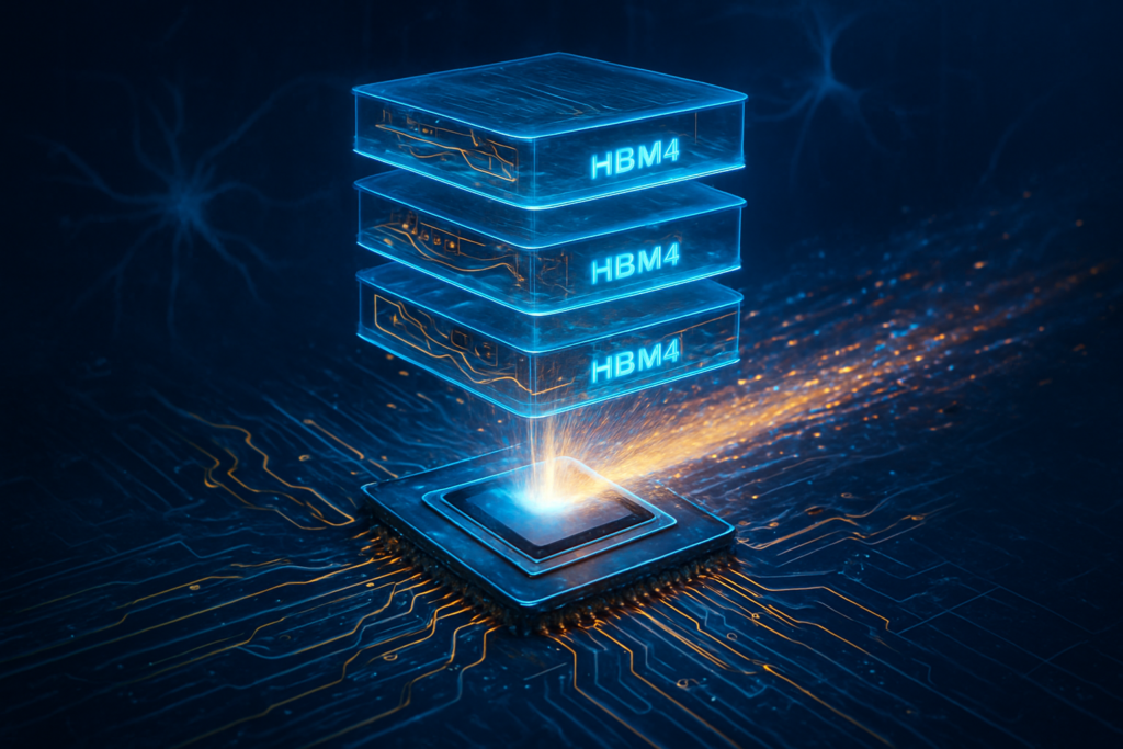
The technical leap from HBM3e to HBM4 is not merely an incremental speed boost; it is a structural redesign. While HBM3e utilized a 1024-bit interface, HBM4 doubles this to a 2048-bit interface, allowing for a massive surge in data throughput without a proportional increase in power consumption. This doubling of the "bus width" is what enables NVIDIA’s new Rubin GPUs to achieve an aggregate bandwidth of 22 TB/s—nearly triple that of the previous Blackwell generation. Furthermore, HBM4 introduces 16-layer (16-Hi) stacking, pushing individual stack capacities to 64GB and allowing a single GPU to house up to 288GB of high-speed VRAM.
Perhaps the most radical departure from previous generations is the shift to a "logic-based" base die. Historically, the base die of an HBM stack was manufactured using a standard DRAM process. In the HBM4 generation, this base die is being fabricated using advanced logic processes—specifically 5nm and 3nm nodes from Taiwan Semiconductor Manufacturing Company (NYSE: TSM) and Samsung’s own foundry. By integrating logic into the memory stack, manufacturers can now perform "near-memory processing," such as offloading Key-Value (KV) cache tasks directly into the HBM. This reduces the constant back-and-forth traffic between the memory and the GPU, significantly lowering the "latency tax" that has historically slowed down LLM inference.
Initial reactions from the AI research community have been electric. Industry experts note that the move to Hybrid Bonding—a copper-to-copper connection method that replaces traditional solder bumps—has allowed for thinner stacks with superior thermal characteristics. "We are finally seeing the hardware catch up to the theoretical requirements of the next generation of foundational models," said one senior researcher at a major AI lab. "HBM4 isn't just faster; it's smarter. It allows us to treat the entire memory pool as a unified, active compute fabric."
The competitive landscape of the semiconductor industry is being redrawn by these developments. SK Hynix, currently the market leader, has solidified its position through a "One-Team" alliance with TSMC. By leveraging TSMC’s advanced CoWoS (Chip-on-Wafer-on-Substrate) packaging and logic dies, SK Hynix has managed to bring HBM4 to mass production six months ahead of its original 2026 schedule. This strategic partnership has allowed them to capture an estimated 70% of the initial HBM4 orders for NVIDIA’s Rubin rollout, positioning them as the primary beneficiary of the AI memory supercycle.
Samsung Electronics, meanwhile, is betting on its unique position as the world's only company that can provide a "turnkey" solution—designing the DRAM, fabricating the logic die in its own 4nm foundry, and handling the final packaging. Despite trailing SK Hynix in the HBM3e cycle, Samsung’s massive $20 billion investment in HBM4 capacity at its Pyeongtaek facility signals a fierce comeback attempt. Micron Technology has also emerged as a formidable contender, with CEO Sanjay Mehrotra confirming that the company's 2026 HBM4 supply is already fully booked. Micron’s expansion into the United States, supported by billions in CHIPS Act grants, provides a strategic advantage for Western tech giants looking to de-risk their supply chains from East Asian geopolitical tensions.
The implications for AI startups and major labs like OpenAI and Anthropic are profound. The availability of HBM4-equipped hardware will likely dictate the "training ceiling" for the next two years. Companies that secured early allocations of Rubin GPUs will have a distinct advantage in training models with 10 to 50 times the complexity of GPT-4. Conversely, the high cost and chronic undersupply of HBM4—which is expected to persist through the end of 2026—could create a wider "compute divide," where only the most well-funded organizations can afford the hardware necessary to stay at the frontier of AI research.
Looking at the broader AI landscape, the HBM4 transition is the clearest evidence yet that we have moved past the "software-only" phase of the AI revolution. The "Memory Wall"—the phenomenon where processor performance increases faster than memory bandwidth—has been the primary inhibitor of AI scaling for years. By effectively breaching this wall, HBM4 enables the transition from "dense" models to "sparse" Mixture-of-Experts (MoE) architectures that can handle hundreds of trillions of parameters. This is the hardware foundation required for the "Agentic AI" era, where models must maintain massive contexts of data to perform complex, multi-step reasoning.
However, this progress comes with significant concerns. The sheer cost of HBM4—driven by the complexity of hybrid bonding and logic-die integration—is pushing the price of flagship AI accelerators toward the $50,000 to $70,000 range. This hyper-inflation of hardware costs raises questions about the long-term sustainability of the AI boom and the potential for a "bubble" if the ROI on these massive investments doesn't materialize quickly. Furthermore, the concentration of HBM4 production in just three companies creates a single point of failure for the global AI economy, a vulnerability that has prompted the U.S., South Korea, and Japan to enter into unprecedented "Technology Prosperity" deals to secure and subsidize these facilities.
Comparisons are already being made to previous semiconductor milestones, such as the introduction of EUV (Extreme Ultraviolet) lithography. Like EUV, HBM4 is seen as a "gatekeeper technology"—those who master it define the limits of what is possible in computing. The transition also highlights a shift in geopolitical strategy; the U.S. government’s decision to finalize nearly $7 billion in grants for Micron and SK Hynix’s domestic facilities in late 2025 underscores that memory is now viewed as a matter of national security, on par with the most advanced logic chips.
The road ahead for HBM is already being paved. Even as HBM4 begins its first volume shipments in early 2026, the industry is already looking toward HBM4e and HBM5. Experts predict that by 2027, we will see the integration of optical interconnects directly into the memory stack, potentially using silicon photonics to move data at the speed of light. This would eliminate the electrical resistance that currently limits bandwidth and generates heat, potentially allowing for 100 TB/s systems by the end of the decade.
The next major challenge to be addressed is the "Power Wall." As HBM stacks grow taller and GPUs consume upwards of 1,000 watts, managing the thermal density of these systems will require a transition to liquid cooling as a standard requirement for data centers. We also expect to see the rise of "Custom HBM," where companies like Google (Alphabet Inc. – NASDAQ: GOOGL) or Amazon (Amazon.com, Inc. – NASDAQ: AMZN) commission bespoke memory stacks with specialized logic dies tailored specifically for their proprietary AI chips (TPUs and Trainium). This move toward vertical integration will likely be the next frontier of competition in the 2026–2030 window.
The HBM4 transition marks the official beginning of the "Memory-First" era of computing. By doubling bandwidth, integrating logic directly into the memory stack, and attracting tens of billions of dollars in strategic investment, HBM4 has become the essential scaffolding for the next generation of artificial intelligence. The announcements at CES 2026 have made it clear: the race for AI supremacy is no longer just about who has the fastest processor, but who can most efficiently move the massive oceans of data required to make those processors "think."
As we look toward the rest of 2026, the industry will be watching the yield rates of hybrid bonding and the successful integration of TSMC’s logic dies into SK Hynix and Samsung’s stacks. The "Memory Supercycle" is no longer a theoretical prediction—it is a $100 billion reality that is reshaping the global economy. For AI to reach its next milestone, it must first overcome its physical limits, and HBM4 is the bridge that will take it there.
This content is intended for informational purposes only and represents analysis of current AI developments.
TokenRing AI delivers enterprise-grade solutions for multi-agent AI workflow orchestration, AI-powered development tools, and seamless remote collaboration platforms.
For more information, visit https://www.tokenring.ai/.