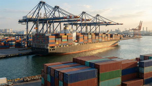


In a move set to significantly reshape the global semiconductor landscape, Taiwan Semiconductor Manufacturing Company (TSMC) (NYSE: TSM), the world's largest contract chipmaker, has been reportedly exploring the establishment of an advanced packaging production facility in Japan. While specific details regarding scale and timeline remain under wraps as of reports circulating in March 2024, this strategic initiative underscores a critical push towards diversifying the semiconductor supply chain and bolstering advanced manufacturing capabilities outside of Taiwan. This potential expansion, distinct from TSMC's existing advanced packaging R&D center in Ibaraki, represents a pivotal moment for high-performance computing and artificial intelligence, promising to enhance the resilience and efficiency of chip production for the most cutting-edge technologies.
The reported plans signal a proactive response to escalating geopolitical tensions and the lessons learned from recent supply chain disruptions, aiming to de-risk the concentration of advanced chip manufacturing. By bringing its sophisticated Chip on Wafer on Substrate (CoWoS) technology to Japan, TSMC is not only securing its own future but also empowering Japan's ambitions to revitalize its domestic semiconductor industry. This development is poised to have immediate and far-reaching implications for AI innovation, enabling more robust and distributed production of the specialized processors that power the next generation of intelligent systems.
The Dawn of Distributed Advanced Packaging: CoWoS Comes to Japan
The proposed advanced packaging facility in Japan is anticipated to be a hub for TSMC's proprietary Chip on Wafer on Substrate (CoWoS) technology. CoWoS is a revolutionary 2.5D/3D wafer-level packaging technique that allows for the stacking of multiple chips, such as logic processors and high-bandwidth memory (HBM), onto an interposer. This intricate process facilitates significantly higher data transfer rates and greater integration density compared to traditional 2D packaging, making it indispensable for advanced AI accelerators, high-performance computing (HPC) processors, and graphics processing units (GPUs). Currently, the bulk of TSMC's CoWoS capacity resides in Taiwan, a concentration that has raised concerns given the surging global demand for AI chips.
This move to Japan represents a significant geographical diversification for CoWoS production. Unlike previous approaches that largely centralized such advanced processes, TSMC's potential Japanese facility would distribute this critical capability, mitigating risks associated with natural disasters, geopolitical instability, or other unforeseen disruptions in a single region. The technical implications are profound: it means a more robust pipeline for delivering the foundational hardware for AI development. Initial reactions from the AI research community and industry experts have been overwhelmingly positive, emphasizing the enhanced supply security this could bring to the development of next-generation AI models and applications, which are increasingly reliant on these highly integrated, powerful chips.
The differentiation from existing technology lies primarily in the strategic decentralization of a highly specialized and bottlenecked manufacturing step. While TSMC has established front-end fabs in Japan (JASM 1 and JASM 2 in Kyushu), bringing advanced packaging, particularly CoWoS, closer to these fabrication sites or to a strong materials and equipment ecosystem in Japan creates a more vertically integrated and resilient regional supply chain. This is a crucial step beyond simply producing wafers, addressing the equally complex and critical final stages of chip manufacturing that often dictate overall system performance and availability.
Reshaping the AI Hardware Landscape: Winners and Competitive Shifts
The establishment of an advanced packaging facility in Japan by TSMC stands to significantly benefit a wide array of AI companies, tech giants, and startups. Foremost among them are companies heavily invested in high-performance AI, such as NVIDIA (NASDAQ: NVDA), Advanced Micro Devices (NASDAQ: AMD) (NASDAQ: AMD), and other developers of AI accelerators that rely on TSMC's CoWoS technology for their cutting-edge products. A diversified and more resilient CoWoS supply chain means these companies can potentially face fewer bottlenecks and enjoy greater stability in securing the packaged chips essential for their AI platforms, from data center GPUs to specialized AI inference engines.
The competitive implications for major AI labs and tech companies are substantial. Enhanced access to advanced packaging capacity could accelerate the development and deployment of new AI hardware. Companies like Google (NASDAQ: GOOGL), Amazon (NASDAQ: AMZN), and Microsoft (NASDAQ: MSFT), all of whom are developing their own custom AI chips or heavily utilizing third-party accelerators, stand to benefit from a more secure and efficient supply of these components. This could lead to faster innovation cycles and a more competitive landscape in AI hardware, potentially disrupting existing products or services that have been hampered by packaging limitations.
Market positioning and strategic advantages will shift as well. Japan's robust ecosystem of semiconductor materials and equipment suppliers, coupled with government incentives, makes it an attractive location for such an investment. This move could solidify TSMC's position as the indispensable partner for advanced AI chip production, while simultaneously bolstering Japan's role in the global semiconductor value chain. For startups in AI hardware, a more reliable supply of advanced packaged chips could lower barriers to entry and accelerate their ability to bring innovative solutions to market, fostering a more dynamic and diverse AI ecosystem.
Broader Implications: A New Era of Supply Chain Resilience
This strategic move by TSMC fits squarely into the broader AI landscape and ongoing trends towards greater supply chain resilience and geographical diversification in advanced technology manufacturing. The COVID-19 pandemic and recent geopolitical tensions have starkly highlighted the vulnerabilities of highly concentrated supply chains, particularly in critical sectors like semiconductors. By establishing advanced packaging capabilities in Japan, TSMC is not just expanding its capacity but actively de-risking the entire ecosystem that underpins modern AI. This initiative aligns with global efforts by various governments, including the US and EU, to foster domestic or allied-nation semiconductor production.
The impacts extend beyond mere supply security. This facility will further integrate Japan into the cutting edge of semiconductor manufacturing, leveraging its strengths in materials science and precision engineering. It signals a renewed commitment to collaborative innovation between leading technology nations. Potential concerns, while fewer than the benefits, might include the initial costs and complexities of setting up such an advanced facility, as well as the need for a skilled workforce. However, Japan's government is proactively addressing these through substantial subsidies and educational initiatives.
Comparing this to previous AI milestones, this development may not be a breakthrough in AI algorithms or models, but it is a critical enabler for their continued advancement. Just as the invention of the transistor or the development of powerful GPUs revolutionized computing, the ability to reliably and securely produce the highly integrated chips required for advanced AI is a foundational milestone. It represents a maturation of the infrastructure necessary to support the exponential growth of AI, moving beyond theoretical advancements to practical, large-scale deployment. This is about building the robust arteries through which AI innovation can flow unimpeded.
The Road Ahead: Anticipating Future AI Hardware Innovations
Looking ahead, the establishment of TSMC's advanced packaging facility in Japan is expected to catalyze a cascade of near-term and long-term developments in the AI hardware landscape. In the near term, we can anticipate a gradual easing of supply constraints for high-performance AI chips, particularly those utilizing CoWoS technology. This improved availability will likely accelerate the development and deployment of more sophisticated AI models, as developers gain more reliable access to the necessary computational power. We may also see increased investment from other semiconductor players in diversifying their own advanced packaging operations, inspired by TSMC's strategic move.
Potential applications and use cases on the horizon are vast. With a more robust supply chain for advanced packaging, industries such as autonomous vehicles, advanced robotics, quantum computing, and personalized medicine, all of which heavily rely on cutting-edge AI, could see faster innovation cycles. The ability to integrate more powerful and efficient AI accelerators into smaller form factors will also benefit edge AI applications, enabling more intelligent devices closer to the data source. Experts predict a continued push towards heterogeneous integration, where different types of chips (e.g., CPU, GPU, specialized AI accelerators, memory) are seamlessly integrated into a single package, and Japan's advanced packaging capabilities will be central to this trend.
However, challenges remain. The semiconductor industry is capital-intensive and requires a highly skilled workforce. Japan will need to continue investing in talent development and maintaining a supportive regulatory environment to sustain this growth. Furthermore, as AI models become even more complex, the demands on packaging technology will continue to escalate, requiring continuous innovation in materials, thermal management, and interconnect density. What experts predict will happen next is a stronger emphasis on regional semiconductor ecosystems, with countries like Japan playing a more prominent role in the advanced stages of chip manufacturing, fostering a more distributed and resilient global technology infrastructure.
A New Pillar for AI's Foundation
TSMC's reported move to establish an advanced packaging facility in Japan marks a significant inflection point in the global semiconductor industry and, by extension, the future of artificial intelligence. The key takeaway is the strategic imperative of supply chain diversification, moving critical advanced manufacturing capabilities beyond a single geographical concentration. This initiative not only enhances the resilience of the global tech supply chain but also significantly bolsters Japan's re-emergence as a pivotal player in high-tech manufacturing, particularly in the advanced packaging domain crucial for AI.
This development's significance in AI history cannot be overstated. While not a direct AI algorithm breakthrough, it is a fundamental infrastructure enhancement that underpins and enables all future AI advancements requiring high-performance, integrated hardware. It addresses a critical bottleneck that, if left unaddressed, could have stifled the exponential growth of AI. The long-term impact will be a more robust, distributed, and secure foundation for AI development and deployment worldwide, reducing vulnerability to geopolitical risks and localized disruptions.
In the coming weeks and months, industry watchers will be keenly observing for official announcements regarding the scale, timeline, and specific location of this facility. The execution of this plan will be a testament to the collaborative efforts between TSMC and the Japanese government. This initiative is a powerful signal that the future of advanced AI will be built not just on groundbreaking algorithms, but also on a globally diversified and resilient manufacturing ecosystem capable of delivering the most sophisticated hardware.
This content is intended for informational purposes only and represents analysis of current AI developments.
TokenRing AI delivers enterprise-grade solutions for multi-agent AI workflow orchestration, AI-powered development tools, and seamless remote collaboration platforms.
For more information, visit https://www.tokenring.ai/.