

The relentless pursuit of artificial intelligence and high-performance computing (HPC) is ushering in a new era of semiconductor manufacturing, pushing the boundaries of what's possible in chip design and production. Far beyond simply shrinking transistors, the industry is now deploying a sophisticated arsenal of novel processes, advanced materials, and ingenious packaging techniques to deliver the powerful, energy-efficient chips demanded by today's complex AI models and data-intensive workloads. This multi-faceted revolution is not just an incremental step but a fundamental shift, promising to accelerate the AI landscape in ways previously unimaginable.
As of October 2nd, 2025, the impact of these breakthroughs is becoming increasingly evident, with major foundries and chip designers racing to implement technologies that redefine performance metrics. From atomic-scale transistor architectures to three-dimensional chip stacking, these innovations are laying the groundwork for the next generation of AI accelerators, cloud infrastructure, and intelligent edge devices, ensuring that the exponential growth of AI continues unabated.
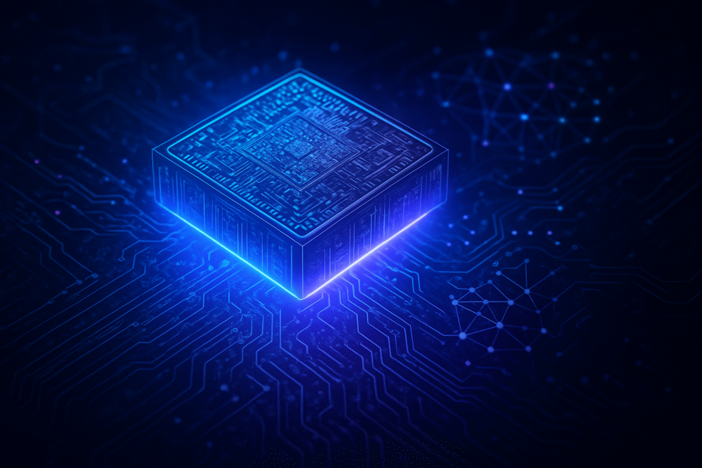
Engineering the Future: A Deep Dive into Semiconductor Advancements
The core of this silicon revolution lies in several transformative technical advancements that are collectively overcoming the physical limitations of traditional chip scaling.
One of the most significant shifts is the transition from FinFET transistors to Gate-All-Around FETs (GAAFETs), often referred to as Multi-Bridge Channel FETs (MBCFETs) by Samsung (KRX: 005930). For over a decade, FinFETs have been the workhorse of advanced nodes, but GAAFETs, now central to 3nm and 2nm technologies, offer superior electrostatic control over the transistor channel, leading to higher transistor density and dramatically improved power efficiency. Samsung has already commercialized its second-generation 3nm GAA technology in 2025, while TSMC (NYSE: TSM) anticipates its 2nm (N2) process, featuring GAAFETs, will enter mass production this year, with commercial chips expected in early 2026. Intel (NASDAQ: INTC) is also leveraging its RibbonFET transistors, its GAA implementation, within its cutting-edge 18A node.
Complementing these new transistor architectures is the groundbreaking Backside Power Delivery Network (BSPDN). Traditionally, power and signal lines share the front side of the wafer, leading to congestion and efficiency losses. BSPDN ingeniously relocates the power delivery network to the backside, freeing up valuable front-side real estate for signal routing. This innovation significantly reduces resistance and parasitic voltage (IR) drop, allowing for thicker, lower-resistance power lines that boost power efficiency, enhance performance, and offer greater design flexibility. Intel's PowerVia is already being implemented at its 18A node, and TSMC plans to integrate its Super PowerRail architecture in its A16 node by 2025. Samsung is optimizing its 2nm process for BSPDN, targeting mass production by 2027, with projections of substantial improvements in chip size, performance, and power efficiency.
Driving the ability to etch these minuscule features is High-Numerical Aperture (High-NA) Extreme Ultraviolet (EUV) lithography. Tools like ASML's (NASDAQ: ASML) TWINSCAN EXE:5000 and EXE:5200B are indispensable for manufacturing features smaller than 2 nanometers. These systems achieve an unprecedented 8 nm resolution with a single exposure, a massive leap from the 13 nm of previous EUV generations, enabling nearly three times greater transistor density. Early adopters like Intel are using High-NA EUV to simplify complex manufacturing and improve yields, targeting risk production on its 14A process in 2027. SK Hynix has also adopted High-NA EUV for mass production, accelerating memory development for AI and HPC.
Beyond processes, new materials are also playing a crucial role. AI itself is being employed to design novel compound semiconductors that promise enhanced performance, faster processing, and greater energy efficiency. Furthermore, advanced packaging materials, such as glass core substrates, are enabling sophisticated integration techniques. The burgeoning demand for High-Bandwidth Memory (HBM), with HBM3 and HBM3e widely adopted and HBM4 anticipated in late 2025, underscores the critical need for specialized memory materials to feed hungry AI accelerators.
Finally, advanced packaging and heterogeneous integration have emerged as cornerstones of innovation, particularly as traditional transistor scaling slows. Techniques like 2.5D and 3D integration/stacking are transforming chip architecture. 2.5D packaging, exemplified by TSMC's Chip-on-Wafer-on-Substrate (CoWoS) and Intel's Embedded Multi-die Interconnect Bridge (EMIB), places multiple dies side-by-side on an interposer for high-bandwidth communication. More revolutionary is 3D integration, which vertically stacks active dies, drastically reducing interconnect lengths and boosting performance. The 3D stacking market, valued at $8.2 billion in 2024, is driven by the need for higher-density chips that cut latency and power consumption. TSMC is aggressively expanding its CoWoS and System on Integrated Chips (SoIC) capacity, while AMD's (NASDAQ: AMD) EPYC processors with 3D V-Cache technology demonstrate significant performance gains by stacking SRAM on top of CPU chiplets. Hybrid bonding is a fundamental technique enabling ultra-fine interconnect pitches, combining dielectric and metal bonding at the wafer level for superior electrical performance. The rise of chiplets and heterogeneous integration allows for combining specialized dies from various process nodes into a single package, optimizing for performance, power, and cost. Companies like AMD (e.g., Instinct MI300) and NVIDIA (NASDAQ: NVDA) (e.g., Grace Hopper Superchip) are already leveraging this to create powerful, unified packages for AI and HPC. Emerging techniques like Co-Packaged Optics (CPO), integrating photonic and electronic ICs, and Panel-Level Packaging (PLP) for cost-effective, large-scale production, further underscore the breadth of this packaging revolution.
Reshaping the AI Landscape: Corporate Impact and Competitive Edges
These advancements are profoundly impacting the competitive dynamics among AI companies, tech giants, and ambitious startups, creating clear beneficiaries and potential disruptors.
Leading foundries like TSMC (NYSE: TSM) and Samsung (KRX: 005930) stand to gain immensely, as they are at the forefront of developing and commercializing the 2nm/3nm GAAFET processes, BSPDN, and advanced packaging solutions like CoWoS and SoIC. Their ability to deliver these cutting-edge technologies is critical for major AI chip designers. Similarly, Intel (NASDAQ: INTC), with its aggressive roadmap for 18A and 14A nodes featuring RibbonFETs, PowerVia, and early adoption of High-NA EUV, is making a concerted effort to regain its leadership in process technology, directly challenging its foundry rivals.
Chip design powerhouses such as NVIDIA (NASDAQ: NVDA) and AMD (NASDAQ: AMD) are direct beneficiaries. The ability to access smaller, more efficient transistors, coupled with advanced packaging techniques, allows them to design increasingly powerful and specialized AI accelerators (GPUs, NPUs) that are crucial for training and inference of large language models and complex AI applications. Their adoption of heterogeneous integration and chiplet architectures, as seen in NVIDIA's Grace Hopper Superchip and AMD's Instinct MI300, demonstrates how these manufacturing breakthroughs translate into market-leading products. This creates a virtuous cycle where demand from these AI leaders fuels further investment in manufacturing innovation.
The competitive implications are significant. Companies that can secure access to the most advanced nodes and packaging technologies will maintain a strategic advantage in performance, power efficiency, and time-to-market for their AI solutions. This could lead to a widening gap between those with privileged access and those relying on older technologies. Startups with innovative AI architectures may find themselves needing to partner closely with leading foundries or invest heavily in design optimization for advanced packaging to compete effectively. Existing products and services, especially in cloud computing and edge AI, will see continuous upgrades in performance and efficiency, potentially disrupting older hardware generations and accelerating the adoption of new AI capabilities. The market positioning of major AI labs and tech companies will increasingly hinge not just on their AI algorithms, but on their ability to leverage the latest silicon innovations.
Broader Significance: Fueling the AI Revolution
The advancements in semiconductor manufacturing are not merely technical feats; they are foundational pillars supporting the broader AI landscape and its rapid evolution. These breakthroughs directly address critical bottlenecks that have historically limited AI's potential, fitting perfectly into the overarching trend of pushing AI capabilities to unprecedented levels.
The most immediate impact is on computational power and energy efficiency. Smaller transistors, GAAFETs, and BSPDN enable significantly higher transistor densities and lower power consumption per operation. This is crucial for training ever-larger AI models, such as multi-modal large language models, which demand colossal computational resources and consume vast amounts of energy. By making individual operations more efficient, these technologies make complex AI tasks more feasible and sustainable. Furthermore, advanced packaging, especially 2.5D and 3D stacking, directly tackles the "memory wall" problem by dramatically increasing bandwidth between processing units and memory. This is vital for AI workloads that are inherently data-intensive and memory-bound, allowing AI accelerators to process information much faster and more efficiently.
These advancements also enable greater specialization. The chiplet approach, combined with heterogeneous integration, allows designers to combine purpose-built processing units (CPUs, GPUs, AI accelerators, custom logic) into a single, optimized package. This tailored approach is essential for specific AI tasks, from real-time inference at the edge to massive-scale training in data centers, leading to systems that are not just faster, but fundamentally better suited to AI's diverse demands. The symbiotic relationship where AI helps design these complex chips (AI-driven EDA tools) and these chips, in turn, power more advanced AI, highlights a self-reinforcing cycle of innovation.
Comparisons to previous AI milestones reveal the magnitude of this moment. Just as the development of GPUs catalyzed deep learning, and the proliferation of cloud computing democratized access to AI resources, the current wave of semiconductor innovation is setting the stage for the next leap. It's enabling AI to move beyond theoretical models into practical, scalable, and increasingly intelligent applications across every industry. While the potential benefits are immense, concerns around the environmental impact of increased chip production, the concentration of manufacturing power, and the ethical implications of ever-more powerful AI systems will continue to be important considerations as these technologies proliferate.
The Road Ahead: Future Developments and Expert Predictions
The current wave of semiconductor innovation is merely a prelude to even more transformative developments on the horizon, promising to further reshape the capabilities of AI.
In the near term, we can expect continued refinement and mass production ramp-up of the 2nm and A16 nodes, with major foundries pushing for even denser and more efficient processes. The widespread adoption of High-NA EUV will become standard for leading-edge manufacturing, simplifying complex lithography steps. We will also see the full commercialization of HBM4 memory in late 2025, providing another significant boost to memory bandwidth for AI accelerators. The chiplet ecosystem will mature further, with standardized interfaces and more collaborative design environments, making heterogeneous integration accessible to a broader range of companies and applications.
Looking further out, experts predict the emergence of even more exotic materials beyond silicon, such as 2D materials (e.g., graphene, MoS2) for ultra-thin transistors and potentially even new forms of computing like neuromorphic or quantum computing, though these are still largely in research phases. The integration of advanced cooling solutions directly into chip packages, possibly through microchannels and direct liquid cooling, will become essential as power densities continue to climb. Furthermore, the role of AI in chip design and manufacturing will deepen, with AI-driven electronic design automation (EDA) tools becoming indispensable for navigating the immense complexity of future chip architectures, accelerating design cycles, and improving yields.
Potential applications on the horizon include truly autonomous systems that can learn and adapt in real-time with unprecedented efficiency, hyper-personalized AI experiences, and breakthroughs in scientific discovery powered by exascale AI and HPC systems. Challenges remain, particularly in managing the thermal output of increasingly dense chips, ensuring supply chain resilience, and the enormous capital investment required for next-generation fabs. However, experts broadly agree that the trajectory points towards an era of pervasive, highly intelligent AI, seamlessly integrated into our daily lives and driving scientific and technological progress at an accelerated pace.
A New Era of Silicon: The Foundation of Tomorrow's AI
In summary, the semiconductor industry is undergoing a profound transformation, moving beyond traditional scaling to a multi-pronged approach that combines revolutionary processes, advanced materials, and sophisticated packaging techniques. Key takeaways include the critical shift to Gate-All-Around (GAA) transistors, the efficiency gains from Backside Power Delivery Networks (BSPDN), the precision of High-NA EUV lithography, and the immense performance benefits derived from 2.5D/3D integration and the chiplet ecosystem. These innovations are not isolated but form a synergistic whole, each contributing to the creation of more powerful, efficient, and specialized chips.
This development marks a pivotal moment in AI history, comparable to the advent of the internet or the mobile computing revolution. It is the bedrock upon which the next generation of artificial intelligence will be built, enabling capabilities that were once confined to science fiction. The ability to process vast amounts of data with unparalleled speed and efficiency will unlock new frontiers in machine learning, robotics, natural language processing, and scientific research.
In the coming weeks and months, watch for announcements from major foundries regarding their 2nm and A16 production ramps, new product launches from chip designers like NVIDIA (NASDAQ: NVDA) and AMD (NASDAQ: AMD) leveraging these technologies, and further advancements in heterogeneous integration and HBM memory. The race for AI supremacy is intrinsically linked to the mastery of silicon, and the current advancements indicate a future where intelligence is not just artificial, but profoundly accelerated by the ingenuity of chip manufacturing.
This content is intended for informational purposes only and represents analysis of current AI developments.
TokenRing AI delivers enterprise-grade solutions for multi-agent AI workflow orchestration, AI-powered development tools, and seamless remote collaboration platforms.
For more information, visit https://www.tokenring.ai/.