

The semiconductor industry stands at a pivotal juncture, grappling with the fundamental limits of traditional transistor scaling that have long propelled technological progress under Moore's Law. As the physical and economic barriers to further miniaturization become increasingly formidable, a paradigm shift is underway, ushering in a revolutionary era for chip architecture. This transformation is not merely an incremental improvement but a fundamental rethinking of how computing systems are designed and built, driven by the insatiable demands of artificial intelligence, high-performance computing, and the ever-expanding intelligent edge.
At the forefront of this architectural revolution are three transformative approaches: chiplets, heterogeneous integration, and neuromorphic computing. These innovations promise to redefine performance, power efficiency, and flexibility, offering pathways to overcome the limitations of monolithic designs and unlock unprecedented capabilities for the next generation of AI and advanced computing. The industry is rapidly moving towards a future where specialized, interconnected, and brain-inspired processing units will power everything from data centers to personal devices, marking a significant departure from the uniform, general-purpose processors of the past.
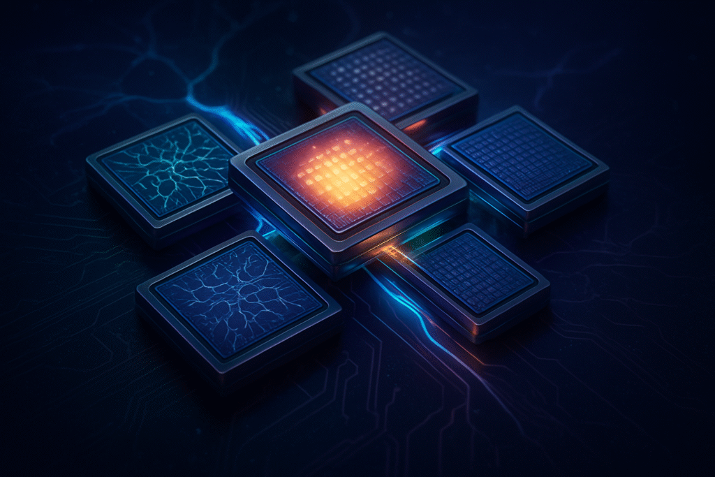
Unpacking the Innovations: Chiplets, Heterogeneous Integration, and Neuromorphic Computing
The future of silicon is no longer solely about shrinking transistors but about smarter assembly and entirely new computational models. Each of these architectural advancements addresses distinct challenges while collectively pushing the boundaries of what's possible in computing.
Chiplets: Modular Powerhouses for Custom Design
Chiplets represent a modular approach where a larger system is composed of multiple smaller, specialized semiconductor dies (chiplets) interconnected within a single package. Unlike traditional monolithic chips that integrate all functionalities onto one large die, chiplets allow for independent development and manufacturing of components such as CPU cores, GPU accelerators, memory controllers, and I/O interfaces. This disaggregated design offers significant advantages: enhanced manufacturing yields due to smaller die sizes being less prone to defects; cost efficiency by allowing the use of advanced, expensive process nodes only for performance-critical chiplets while others utilize more mature, cost-effective nodes; and unparalleled flexibility, enabling manufacturers to mix and match components for highly customized solutions. Companies like Intel Corporation (NASDAQ: INTC) and Advanced Micro Devices (NASDAQ: AMD) have been early adopters, utilizing chiplet designs in their latest processors to achieve higher core counts and specialized functionalities. The nascent Universal Chiplet Interconnect Express (UCIe) consortium, backed by industry giants, aims to standardize chiplet interfaces, promising to further accelerate their adoption and interoperability.
Heterogeneous Integration: Weaving Diverse Technologies Together
Building upon the chiplet concept, heterogeneous integration (HI) takes advanced packaging to the next level by combining different semiconductor components—often chiplets—made from various materials or using different process technologies into a single, cohesive package or System-in-Package (SiP). This allows for the seamless integration of diverse functionalities like logic, memory, power management, RF, and photonics. HI is critical for overcoming the physical constraints of monolithic designs by enabling greater functional density, faster chip-to-chip communication, and lower latency through advanced packaging techniques such as 2.5D (e.g., using silicon interposers) and 3D integration (stacking dies vertically). This approach allows designers to optimize products at the system level, leading to significant boosts in performance and reductions in power consumption for demanding applications like AI accelerators and 5G infrastructure. Companies like Taiwan Semiconductor Manufacturing Company (NYSE: TSM) are at the forefront of developing sophisticated HI technologies, offering advanced packaging solutions like CoWoS (Chip-on-Wafer-on-Substrate) that are crucial for high-performance AI chips.
Neuromorphic Computing: The Brain-Inspired Paradigm
Perhaps the most radical departure from conventional computing, neuromorphic computing draws inspiration directly from the human brain's structure and function. Unlike the traditional von Neumann architecture, which separates memory and processing, neuromorphic systems integrate these functions, using artificial neurons and synapses that communicate through "spikes." This event-driven, massively parallel processing paradigm is inherently different from clock-driven, sequential computing. Its primary allure lies in its exceptional energy efficiency, often cited as orders of magnitude more efficient than conventional systems for specific AI workloads, and its ability to perform real-time learning and inference with ultra-low latency. While still in its early stages, research by IBM (NYSE: IBM) with its TrueNorth chip and Intel Corporation (NASDAQ: INTC) with Loihi has demonstrated the potential for neuromorphic chips to excel in tasks like pattern recognition, sensory processing, and continuous learning, making them ideal for edge AI, robotics, and autonomous systems where power consumption and real-time adaptability are paramount.
Reshaping the AI and Tech Landscape: A Competitive Shift
The embrace of chiplets, heterogeneous integration, and neuromorphic computing is poised to dramatically reshape the competitive dynamics across the AI and broader tech industries. Companies that successfully navigate and innovate in these new architectural domains stand to gain significant strategic advantages, while others risk being left behind.
Beneficiaries and Competitive Implications
Major semiconductor firms like Intel Corporation (NASDAQ: INTC) and Advanced Micro Devices (NASDAQ: AMD) are already leveraging chiplet architectures to deliver more powerful and customizable CPUs and GPUs, allowing them to compete more effectively in diverse markets from data centers to consumer electronics. NVIDIA Corporation (NASDAQ: NVDA), a dominant force in AI accelerators, is also heavily invested in advanced packaging and integration techniques to push the boundaries of its GPU performance. Foundry giants like Taiwan Semiconductor Manufacturing Company (NYSE: TSM) are critical enablers, as their advanced packaging technologies are essential for heterogeneous integration. These companies are not just offering manufacturing services but are becoming strategic partners in chip design, providing the foundational technologies for these complex new architectures.
Disruption and Market Positioning
The shift towards modular and integrated designs could disrupt the traditional "fabless" model for some companies, as the complexity of integrating diverse chiplets requires deeper collaboration with foundries and packaging specialists. Startups specializing in specific chiplet functionalities or novel interconnect technologies could emerge as key players, fostering a more fragmented yet innovative ecosystem. Furthermore, the rise of neuromorphic computing, while still nascent, could create entirely new market segments for ultra-low-power AI at the edge. Companies that can develop compelling software and algorithms optimized for these brain-inspired chips could carve out significant niches, potentially challenging the dominance of traditional GPU-centric AI training. The ability to rapidly iterate and customize designs using chiplets will also accelerate product cycles, putting pressure on companies with slower, monolithic design processes.
Strategic Advantages
The primary strategic advantage offered by these architectural shifts is the ability to achieve unprecedented levels of specialization and optimization. Instead of a one-size-fits-all approach, companies can now design chips tailored precisely for specific AI workloads, offering superior performance per watt and cost-effectiveness. This enables tech giants like Alphabet Inc. (NASDAQ: GOOGL) and Meta Platforms, Inc. (NASDAQ: META) to design their own custom AI accelerators, leveraging these advanced packaging techniques to build powerful, domain-specific hardware that gives them a competitive edge in their AI research and deployment. The increased complexity, however, also means that deep expertise in system-level design, thermal management, and robust interconnects will become even more critical, favoring companies with extensive R&D capabilities and strong intellectual property portfolios in these areas.
A New Horizon for AI and Beyond: Broader Implications
These architectural innovations are not merely technical feats; they represent a fundamental shift that will reverberate across the entire AI landscape and beyond, influencing everything from energy consumption to the very nature of intelligent systems.
Fitting into the Broader AI Landscape
The drive for chiplets, heterogeneous integration, and neuromorphic computing is directly intertwined with the explosive growth and increasing sophistication of artificial intelligence. As AI models grow larger and more complex, demanding exponentially more computational power and memory bandwidth, traditional chip designs are becoming bottlenecks. These new architectures provide the necessary horsepower and efficiency to train and deploy advanced AI models, from large language models to complex perception systems in autonomous vehicles. They enable the creation of highly specialized AI accelerators that can perform specific tasks with unparalleled speed and energy efficiency, moving beyond general-purpose CPUs and GPUs for many AI inference workloads.
Impacts: Performance, Efficiency, and Accessibility
The most immediate and profound impact will be on performance and energy efficiency. Chiplets and heterogeneous integration allow for denser, faster, and more power-efficient systems, pushing the boundaries of what's achievable in high-performance computing and data centers. This translates into faster AI model training, quicker inference times, and the ability to deploy more sophisticated AI at the edge. Neuromorphic computing, in particular, promises orders of magnitude improvements in energy efficiency for certain tasks, making AI more accessible in resource-constrained environments like mobile devices, wearables, and ubiquitous IoT sensors. This democratization of powerful AI capabilities could lead to a proliferation of intelligent applications in everyday life.
Potential Concerns
Despite the immense promise, these advancements come with their own set of challenges and potential concerns. The increased complexity of designing, manufacturing, and testing systems composed of multiple chiplets from various sources raises questions about cost, yield management, and supply chain vulnerabilities. Standardizing interfaces and ensuring interoperability between chiplets from different vendors will be crucial but remains a significant hurdle. For neuromorphic computing, the biggest challenge lies in developing suitable programming models and algorithms that can fully exploit its unique architecture, as well as finding compelling commercial applications beyond niche research. There are also concerns about the environmental impact of increased chip production and the energy consumption of advanced manufacturing processes, even as the resulting chips become more energy-efficient in operation.
Comparisons to Previous AI Milestones
This architectural revolution can be compared to previous pivotal moments in AI history, such as the advent of GPUs for parallel processing that supercharged deep learning, or the development of specialized TPUs (Tensor Processing Units) by Alphabet Inc. (NASDAQ: GOOGL) for AI workloads. However, the current shift is arguably more fundamental, moving beyond mere acceleration to entirely new ways of building and thinking about computing hardware. It represents a foundational enabler for the next wave of AI breakthroughs, allowing AI to move from being a software-centric field to one deeply intertwined with hardware innovation at every level.
The Road Ahead: Anticipating the Next Wave of Innovation
As of October 2, 2025, the trajectory for chip architecture is set towards greater specialization, integration, and brain-inspired computing. The coming years promise a rapid evolution in these domains, unlocking new applications and pushing the boundaries of intelligent systems.
Expected Near-Term and Long-Term Developments
In the near term, we can expect to see wider adoption of chiplet-based designs across a broader range of processors, not just high-end CPUs and GPUs. The UCIe standard, still relatively new, will likely mature, fostering a more robust ecosystem for chiplet interoperability and enabling smaller players to participate. Heterogeneous integration will become more sophisticated, with advancements in 3D stacking technologies and novel interconnects that allow for even tighter integration of logic, memory, and specialized accelerators. We will also see more domain-specific architectures (DSAs) that are highly optimized for particular AI tasks. In the long term, significant strides are anticipated in neuromorphic computing, moving from experimental prototypes to more commercially viable solutions, possibly in hybrid systems that combine neuromorphic cores with traditional digital processors for specific, energy-efficient AI tasks at the edge. Research into new materials beyond silicon, such as carbon nanotubes and 2D materials, will also continue, potentially offering even greater performance and efficiency gains.
Potential Applications and Use Cases on the Horizon
The applications stemming from these architectural advancements are vast and transformative. Enhanced chiplet designs will power the next generation of supercomputers and cloud data centers, dramatically accelerating scientific discovery and complex AI model training. In the consumer space, more powerful and efficient chiplets will enable truly immersive extended reality (XR) experiences and highly capable AI companions on personal devices. Heterogeneous integration will be crucial for advanced autonomous vehicles, integrating high-speed sensors, real-time AI processing, and robust communication systems into compact, energy-efficient modules. Neuromorphic computing promises to revolutionize edge AI, enabling devices to perform complex learning and inference with minimal power, ideal for pervasive IoT, smart cities, and advanced robotics that can learn and adapt in real-time. Medical diagnostics, personalized healthcare, and even brain-computer interfaces could also see significant advancements.
Challenges That Need to Be Addressed
Despite the exciting prospects, several challenges remain. The complexity of designing, verifying, and testing systems with dozens or even hundreds of interconnected chiplets is immense, requiring new design methodologies and sophisticated EDA (Electronic Design Automation) tools. Thermal management within highly integrated 3D stacks is another critical hurdle. For neuromorphic computing, the biggest challenge is developing a mature software stack and programming paradigms that can fully harness its unique capabilities, alongside creating benchmarks that accurately reflect its efficiency for real-world problems. Standardization across the board – from chiplet interfaces to packaging technologies – will be crucial for broad industry adoption and cost reduction.
What Experts Predict Will Happen Next
Industry experts predict a future characterized by "system-level innovation," where the focus shifts from individual component performance to optimizing the entire computing stack. Dr. Lisa Su, CEO of Advanced Micro Devices (NASDAQ: AMD), has frequently highlighted the importance of modular design and advanced packaging. Jensen Huang, CEO of NVIDIA Corporation (NASDAQ: NVDA), emphasizes the need for specialized accelerators for the AI era. The consensus is that the era of monolithic general-purpose CPUs dominating all workloads is waning, replaced by a diverse ecosystem of specialized, interconnected processors. We will see continued investment in hybrid approaches, combining the strengths of traditional and novel architectures, as the industry progressively moves towards a more heterogeneous and brain-inspired computing future.
The Future is Modular, Integrated, and Intelligent: A New Chapter in AI Hardware
The current evolution in chip architecture, marked by the rise of chiplets, heterogeneous integration, and neuromorphic computing, signifies a monumental shift in the semiconductor industry. This is not merely an incremental step but a foundational re-engineering that addresses the fundamental limitations of traditional scaling and paves the way for the next generation of artificial intelligence and high-performance computing.
Summary of Key Takeaways
The key takeaways are clear: the era of monolithic chip design is giving way to modularity and sophisticated integration. Chiplets offer unprecedented flexibility, cost-efficiency, and customization, allowing for tailored solutions for diverse applications. Heterogeneous integration provides the advanced packaging necessary to weave these specialized components into highly performant and power-efficient systems. Finally, neuromorphic computing, inspired by the brain, promises revolutionary gains in energy efficiency and real-time learning for specific AI workloads. Together, these innovations are breaking down the barriers that Moore's Law once defined, opening new avenues for computational power.
Assessment of This Development's Significance in AI History
This architectural revolution will be remembered as a critical enabler for the continued exponential growth of AI. Just as GPUs unlocked the potential of deep learning, these new chip architectures will provide the hardware foundation for future AI breakthroughs, from truly autonomous systems to advanced human-computer interfaces and beyond. They will allow AI to become more pervasive, more efficient, and more capable than ever before, moving from powerful data centers to the most constrained edge devices. This marks a maturation of the AI field, where hardware innovation is now as crucial as algorithmic advancements.
Final Thoughts on Long-Term Impact
The long-term impact of these developments will be profound. We are moving towards a future where computing systems are not just faster, but fundamentally smarter, more adaptable, and vastly more energy-efficient. This will accelerate progress in fields like personalized medicine, climate modeling, and scientific discovery, while also embedding intelligence seamlessly into our daily lives. The challenges of complexity and standardization are significant, but the industry's collective efforts, as seen with initiatives like UCIe, demonstrate a clear commitment to overcoming these hurdles.
What to Watch For in the Coming Weeks and Months
In the coming weeks and months, keep an eye on announcements from major semiconductor companies regarding new product lines leveraging advanced chiplet designs and 3D packaging. Watch for further developments in industry standards for chiplet interoperability. Additionally, observe the progress of research institutions and startups in neuromorphic computing, particularly in the development of more practical applications and the integration of neuromorphic capabilities into hybrid systems. The ongoing race for AI supremacy will increasingly be fought not just in software, but also in the very silicon that powers it.
This content is intended for informational purposes only and represents analysis of current AI developments.
TokenRing AI delivers enterprise-grade solutions for multi-agent AI workflow orchestration, AI-powered development tools, and seamless remote collaboration platforms.
For more information, visit https://www.tokenring.ai/.